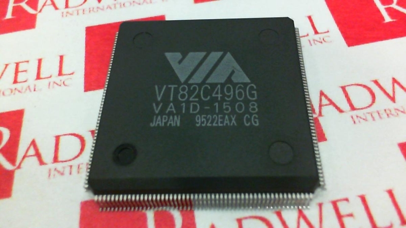
 VIA
VIA
VIA are a motherboard chipset manufacturer for PC compatibles. They also designed and fabricated their own x86-compatible CPUs.
VT82C481, VT82C495An 80386DX chipset that supports chips up to 40 MHz. Believed to also support the Cx486DLC and Texas Instruments TX486DLC CPUs. Motherboards that use this chipset are: |
VT82C486[A], VT82C505Supports level 1 write-back cache. Motherboards that use this chipset are: Award BIOS Chipset codes: 2A4L4 or 214L2 Click here for the 486 datasheet, or here for the 505 datasheet. |
|
Apollo Master (VT82C575M, VT82C576M)In 1995, VIA launched their Apollo Master chipset for socket 5 and 7 motherboards. Bus speeds up to 66 MHz. Apollo Master supports both asynchronous and pipelined burst L2 cache. The VT82C576M is the PCI-to-ISA bridge chip (southbridge), and the VT82C575M is the northbridge. Motherboards that use this chipset are: Click here for the Apollo Master datasheet. |
Apollo Plus (VT82C575MV, VT82C576MV)Similar to Apollo Master (see above), Apollo Plus only supports asynchronous L2 cache. The VT82C576MV is the PCI-to-ISA bridge chip (southbridge), and the VT82C575MV is the northbridge.
|
VP1 (VT82C585VP, VT82C587VP)In 1996, VIA launched their VP1 chipset. Bus speeds from 50 to 66 MHz. Motherboards that used the Apollo VP1 chipset include:
Click here for the Apollo VP1 datasheet. |
VP2 (VT82C595, VT82C586B)In 1997, VIA launched their competitor to Intel's TX chipset. Also called the VP2/97, it was full-featured including support for BEDO and SDRAM, UMA, Ultra DMA. It supported up to 512 MB RAM, all of which was cacheable, plus 2 MB of L2 cache. Processor support ranged from the Pentium, Pentium MMX, AMD K5 and K6, Cyrix 6x86 (M1) and 6x86MX (M2). As with most chipsets of this era, there were two main chips: the VT82C595 (north bridge) and VT82C586B (south bridge). PCI bus speeds supported were 25, 30 and 33 MHz. Main bus speeds were 50, 60 and 66 MHz. Intel's TX chipset had extensive support for power-saving features, and the VIA VP2 followed suit with PC97 compliance. The VP2 stood out with such a rich feature set, nothing else available at the time could beat it. The only thing it didn't support was AGP, which was introduced with the later-released VP3. This chipset was also relabelled as the AMD-640 chipset. Motherboards that used VP2 were:
Click here for the Apollo VP2/VPX/MVP3 datasheet. |
Apollo VP3 (VT82C597)The VIA Apollo VP3 chipset was released in 1996. It was highly anticipated, as it was likely to be the first of the new Super Socket 7 chipsets, i.e. one that supported the new 100 MHz front side bus speed. Unfortunately, when they announced the VP3 chipset they said it would only support FSB speeds up to 66 MHz, but they did say that a 'mobile' version of the VP3, the MVP3, would support the 100 MHz speed + AGP. Increased maximum RAM support to 1 GB. Motherboards that used VP3 were:
Click here for the Apollo VP3 datasheet. |
Apollo MVP3 (VT82C598AT, VT82C586B)The MVP3 chipset was VIA's first true Super 7 chipset, so it supported the 100 MHz front side bus and AGP (Advanced Graphics Processor) slot. Despite the name, the "Mobile" VP3, or MVP3, can be used in both desktop motherboards and laptop motherboards. A direct competitor to the MVP3 was the ALi Aladdin V chipset. The MVP3 differs from the ALi Aladdin V in two areas: Aladdin V only supports EDO, FPM and SDRAM whilst the MVP3 supports DDR (Double Data Rate) SDRAM, and the MVP3 doesn't feature any Tag RAM in its L2 cache. This means that an MVP3 motherboard manufacturer had to include a high quality L2 cache with a fast Tag RAM chip in order to make the 100 MHz FSB speed a stable solution. If the motherboard has 8 or 10 ns SRAM chips, expect to have serious problems at 100 MHz FSB. The MVP3 chipset was also unique in that it enabled memory bus speeds up to 66 MHz while using a 100 MHz FSB speed to derive the processor clock. This means that, in theory, you could even re-use your old generic 60ns EDO SIMMs on a MVP3 motherboard. On the downside, the MVP3 only features an 8-bit integrated Tag comparator, instead of the 10-bit one used on the earlier VP2. This means that only part of the main memory is cacheable (64 MB up to 256 MB) - not the full 1 GB that is supported. CPU support is as follows: AMD K5, K6, K6-3D, Cyrix 6x86 (M1), 6x86MX (MII), Intel Pentium and Pentium MMX. The VIA Apollo MVP3 was loved by overclockers for its ability to desynchronise the FSB from the PCI/ISA/AGP bus but had slightly less good AGP performance than the ALi Aladdin V chipset. The jury's out on whether this was the fastest Super 7 chipset ever - it has a bigger cache over the Aladdin V, but doesn't clock as high. Award BIOS Chipset Code: 6A5LE Motherboards that used MVP3 were:
Click here for the Apollo MVP3 datasheet.
|
Apollo MVP4Award BIOS Chipset Code: 6A5LH (with Award 6.00 BIOS) Motherboards that used MVP4 were: Click here for the Apollo MVP4 datasheet. |
